HALF ADDER - FULL ADDER - MUX
Truth Tables and Verilog Codes for one-bit Half Adder and Full Adder
HALF ADDER
By using half adder, you can design simple addition with the help of logic gates.
 |
| Half Adder |
0+1 = 1
1+0 = 1
1+1 = 10
These are the least possible single-bit combinations. But the result for 1+1 is 10, the sum result must be re-written as a 2-bit output. Thus, the equations can be written as
0+0 = 00
0+1 = 01
1+0 = 01
1+1 = 10
The output ‘1’of ‘10’ is carry-out. ‘SUM’ is the normal output and ‘CARRY’ is the carry-out.
 |
| Half Adder Logic Circuit |
HALF ADDER TRUTH TABLE :

If we want to write Verilog modules
and testbench codes including every possible outcome, for Half Adder and Full
Adder:
HALF ADDER CODE:
module halfandfull(A,B,C,S);
input A,B;
output C,S;
assign C = A^B;
assign S = A&B;
endmodule
HALF ADDER TEST BENCH CODE:
module halffulltb;
reg
A;
reg
B;
wire
C;
wire
S;
halfandfull
uut (
.A(A),
.B(B),
.C(C),
.S(S)
);
initial begin
A
= 0;
B
= 0;
#10;
A
= 0;
B
= 1;
#50;
A
= 1;
B
= 0;
#100;
A
= 1;
B
= 1;
#150;
End
 |
| Half Adder Output |
FULL ADDER
This adder is difficult to implement than a half-adder.
The difference between a half-adder and a full-adder is that the full-adder has three inputs and two outputs, whereas half adder has only two inputs and two outputs.
The first two inputs are A and B and the third input is an input carry as C-IN.
 |
| Full Adder |
The output carry is designated as C-OUT and the normal output is designated as S.
 |
| Full Adder Logic Circuit |
FULL ADDER TRUTH TABLE
S=((A’B+AB’)Cin’)+((A’B+AB’)’Cin)
Cout=((A’B+AB’’)Cin)+AB

FULL ADDER CODE:
module
fulladddder(A,B,Cin,S,Cout);
input A,B,Cin;
output
S,Cout;
assign
S = (A^B)^Cin;
assign
Cout = ((A^B)&Cin) | (A&B) ;
endmodule
FULL ADDER TEST BENCH CODE:
module fulladdertb;
reg
A;
reg
B;
reg
Cin;
wire
S;
wire
Cout;
fulladddder uut (
.A(A),
.B(B),
.Cin(Cin),
.S(S),
.Cout(Cout)
);
initial begin
A
= 0;
B
= 0;
Cin
= 0;
#10;
A
= 0;
B
= 0;
Cin
= 1;
#25;
A
= 0;
B
= 1;
Cin
= 0;
#50;
A=0;
B=1;
Cin =1;
#75;
A=1;
B=0;
Cin=0;
#100;
A=1;
B=0;
Cin=1;
#125;
A=1;
B=1;
Cin=0;
#150;
A=1;
B=1;
Cin=1;
#175
End
Endmodule
 |
| Full Adder Output |
 |
| Full Adder Design Using Half Adders |
MULTIPLEXER
The multiplexer or MUX is a digital switch, also called as data selector.
The multiplexer or MUX is a digital switch, also called as data selector.
Let's write Verilog module code for a 2to1 multiplexer with
inputs 1-bit MuxIn1, 1-bit MuxIn0, 1-bit Slct and output 1-bit MuxOut.

TWOTOONE MUX CODE:
module muxtwotoone(muxin,select,muxout);
input
[1:0] muxin;
input
select;
output reg muxout;
always @(muxin,select)
begin
if(select == 1'b1) muxout = muxin[0];
else if ( select == 1'b0 ) muxout =
muxin[1];
end
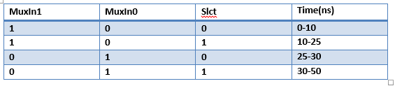
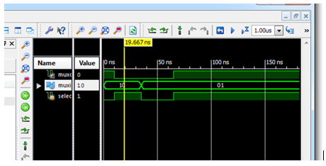
Let's write testbench code for 2 to 1 multiplexer with
respect to the inputs and time intervals given below;
TEST BENCH CODE OF TWOTOONE MUX:
module twotoonetbb;
reg
[1:0] muxin;
reg
select;
wire
muxout;
muxtwotoone
uut (
.muxin(muxin),
.select(select),
.muxout(muxout));
initial begin
muxin
= 2'b10;
select
= 1'b0;
#10;
muxin
= 2'b10;
select
= 1'b1;
#25;
muxin
= 2'b01;
select
= 1'b0;
#30;
muxin
= 2'b01;
select
= 1'b1;
#50;
end
endmodule
Now let's design a 1-bit full adder with 2 to 1 multiplexers
(inverters can be used as well). Draw and include your design in your reports.
M.K.
You can reach VHDL Codes for Full and Half Adder from this site :


Yorumlar
Yorum Gönder